 | –≠–ª–µ–∫—Ç—Ä–æ–Ω–Ω—ã–π –∫–æ–º–ø–æ–Ω–µ–Ω—Ç: THAT1203 | –°–∫–∞—á–∞—Ç—å:  PDF PDF  ZIP ZIP |
THAT Corporation; 45 Sumner Street; Milford, Massachusetts 01757-1656; USA
Tel: +1 508 478 9200; Fax: +1 508 478 0990; Web: www.thatcorp.com
THAT 1200, 1203, 1206
Description
The THAT 1200-series InGenius balanced line
receivers
overcome
a
serious
limitation
of
conventional balanced input stages: poor common
mode rejection in real-world applications. While
conventional input stages measure well in the lab
and perform well on paper, they fail to live up to
their CMRR specs when fed from even slightly
unbalanced source impedances -- a common
situation in almost any pro sound environment.
This is because conventional stages have low
common-mode input impedance, which interacts
with imbalances in source impedance to unbalance
common-mode signals, making them indistin-
guishable from desired, balanced signals.
Developed
by
Bill
Whitlock
of
Jensen
Transformers, the patented InGenius input
stage uses
clever bootstrapping to raise its
common-mode input impedance into the meg-
ohm range without the noise penalty from the
obvious solution of using high-valued resistors.
Like transformers, InGenius line receivers
maintain their high CMRR over a wide range of
source impedance imbalances -- even when fed
from single-ended sources. But unlike trans-
formers, these wide bandwidth solid state de-
vices offer dc-coupling, low distortion, and
transparent sound in a small package at rea-
sonable cost.
T H A T
C o r p o r a t i o n
InGenius High-CMRR
Balanced Input Line Receiver ICs
FEATURES
∑
High CMRR: typ. 90 dB at 60 Hz
∑
Extremely high common-mode input
impedance
∑
Maintains balance under real-world
conditions
∑
Transformer-like performance in an IC
∑
Excellent audio performance
∑
Wide bandwidth: typ. > 22 MHz
∑
High slew rate: typ. 12 V/us
∑
Low distortion: typ. 0.0005 % THD
∑
Low noise: typ. -107 dBu
∑
Several gains: 0 dB, -3 dB, & -6 dB
APPLICATIONS
∑ Balanced Audio Line Receivers
∑ Instrumentation Amplifiers
∑ Differential Amplifiers
∑ Transformer Front-End Replacements
∑ ADC Front-Ends
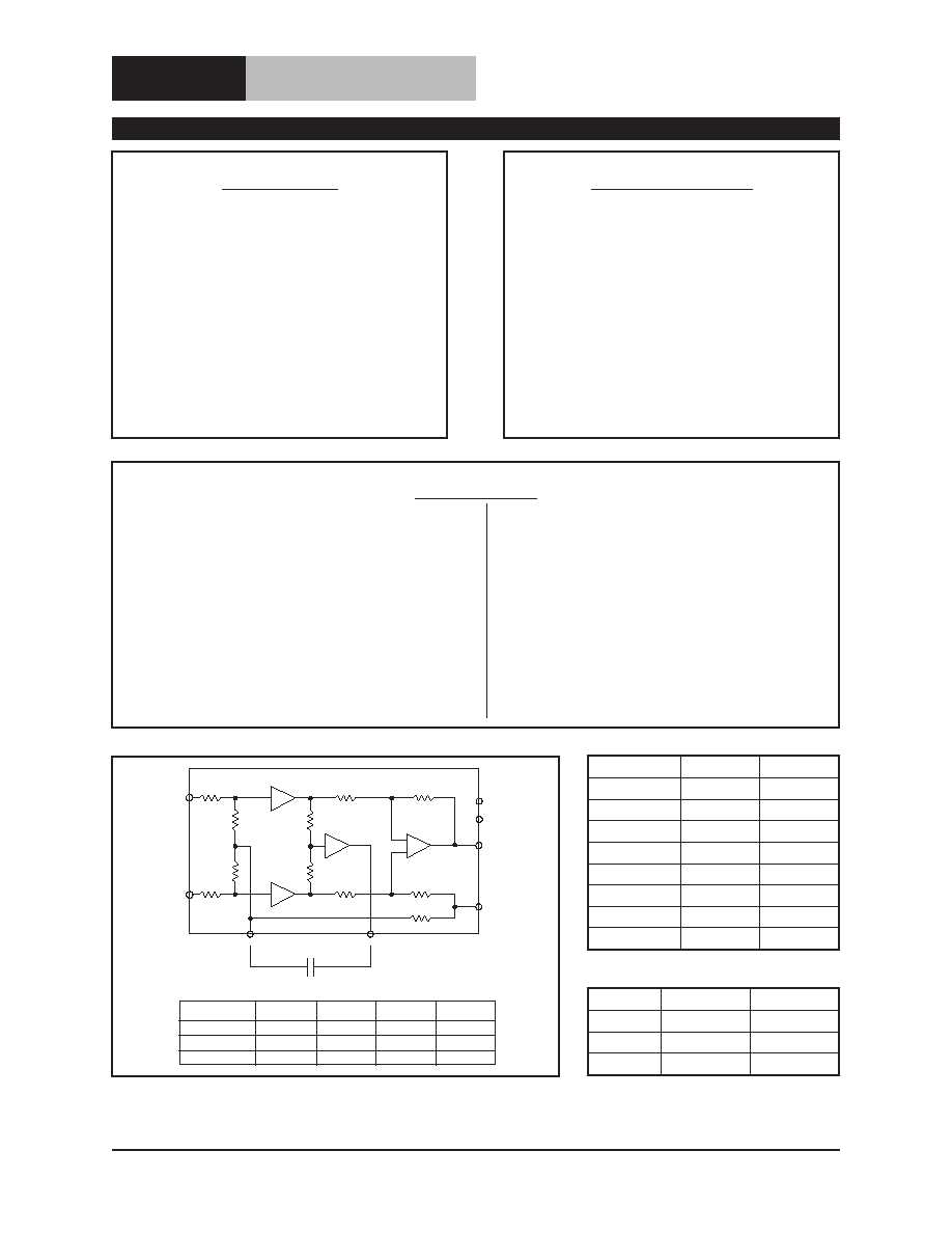
+1
+1
R1
R2
R3
R4
IN-
IN+
REF
CM OUT
Vcc
Vee
Vout
+1
-
+
CM IN
Cb
R5
R7
R8
R10
R11
OA1
OA2
OA3
OA4
Part no.
THAT1200
THAT1203
THAT1206
R2 , R4
6 k
Ÿ
6 Ÿ
5 Ÿ
k
k
R1 , R3
6 k
Ÿ
6 Ÿ
7 Ÿ
k
k
R7 , R8
24 k
Ÿ
17 Ÿ
17 Ÿ
k
k
R6 , R9
0
7 Ÿ
7 Ÿ
k
k
24K
24K
24K
R6
R9
Figure 1. THAT1200-series equivalent circuit diagram
Pin Name
DIP Pin
SO Pin
Ref
1
1
In-
2
2
In+
3
3
Vee
4
4
CM In
5
5
Vout
6
6
Vcc
7
7
CM Out
8
8
Table 1. 1200-series pin assignments
Gain
Plastic DIP
Plastic SO
0 dB
1200P
1200S
-3 dB
1203P
1203S
-6 dB
1206P
1206S
Table 2. Ordering information
Protected under U.S. Patent Numbers, 5,568,561 and 6,160,451. Additional patents pending.
InGenius is a registered trademark of THAT Corporation.
600033 Rev 00

THAT Corporation; 45 Sumner Street; Milford, Massachusetts 01757-1656; USA
Tel: +1 508 478 9200; Fax: +1 508 478 0990; Web: www.thatcorp.com
Page 2
InGenius High-CMRR Balanced Input Line Receiver ICs
Absolute Maximum Ratings (T
A
= 25∞C)
Positive Supply Voltage (V
CC
)
+20 V
Negative Supply Voltage (V
EE
)
-20 V
Storage Temperature Range (T
ST
)
-40 to +125∞C
Output Short-Circuit Duration (t
SH
)
Continuous
Ja
PDIP Pkg
86
∞C/W
Ja
SO Pkg
104
∞C/W
Operating Temperature Range (T
OP
)
0 to +85∞C
Junction Temperature (T
J
)
125∞C
THAT1200
THAT1203
THAT1206
Input Voltage (V
IN
)
± 25 V
± 31 V
± 31 V
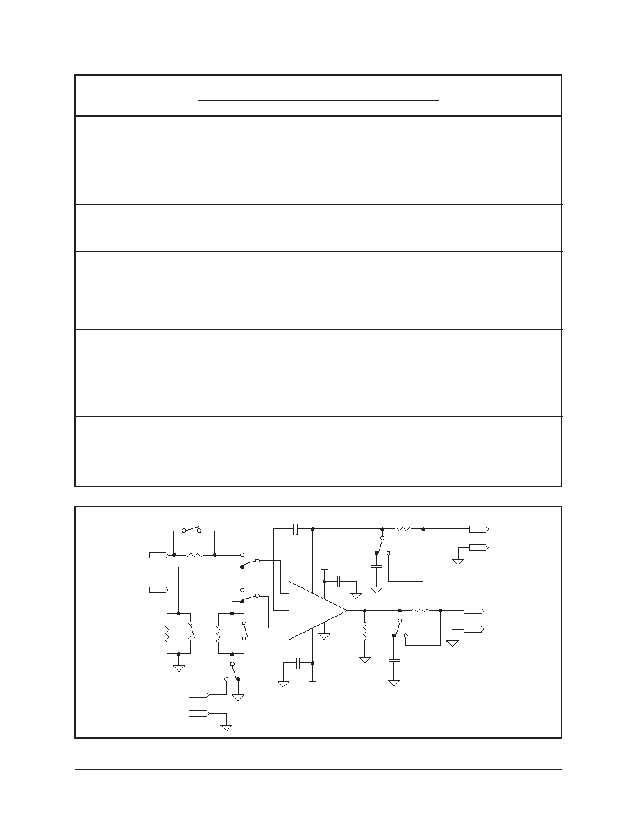
Electrical Characteristics
2 , 3 , 4
Parameter
Symbol
Conditions
Min
Typ
Max
Units
Supply Current
I
CC
No signal
--
4.7
8.0
mA
Supply Voltage
V
CC
, V
EE
±3
±18
V
Input Bias Current
I
B
No signal; Either input
--
700
1,400
nA
connected to GND
Input Offset Current
I
B-OFF
No signal
--
--
±300
nA
Input Voltage Range
V
IN-CM
Common mode
±12.5
±13.0
--
V
V
IN-DIFF
Differential (equal and opposite swing)
THAT 1200
21.0
21.5
--
dBu
THAT 1203
24.0
24.5
--
dBu
THAT 1206
24.0
24.5
--
dBu
Input Impedance
Z
IN-DIFF
Differential
48.0
k
Z
IN-CM
Common mode
with bootstrap
60 Hz
10.0
M
20 kHz
3.2
M
Common Mode Rejection Ratio
CMRR
1
Matched source impedances; V
CM
= ±10V
DC
70
90
--
dB
60 Hz
70
90
--
dB
20 kHz
--
85
--
dB
Common Mode Rejection Ratio
5
CMRR
IEC
10
unmatched source impedances; V
CM
= ±10V
DC
--
90
--
dB
60 Hz
--
90
--
dB
20 kHz
--
85
--
dB
Common Mode Rejection Ratio
CMRR
2
600
unmatched source impedances; V
CM
= ±10V
60 Hz
--
70
--
dB
20 kHz
--
65
--
dB
Power Supply Rejection Ratio
6
PSRR
At 60 Hz, with V
CC
= -V
EE
THAT1200
--
82
--
dB
THAT1203
--
80
--
dB
THAT1206
--
80
--
dB
SPECIFICATIONS
1
1. All specifications are subject to change without notice.
2. Unless otherwise noted, T
A
=25∞C, V
CC
= +15V, V
EE
= -15V
3. See test circuit in Figure 2.
4. 0 dBu = 0.775Vrms.
5. Per IEC Standard 60268-3 for testing CMRR of balanced
inputs.
6. Defined with respect to the differential gain.
THAT Corporation; 45 Sumner Street; Milford, Massachusetts 01757-1656; USA
Tel: +1 508 478 9200; Fax: +1 508 478 0990; Web: www.thatcorp.com
600033 Rev 00
Page 3
Electrical Characteristics (Cont'd)
Parameter
Symbol
Conditions
Min
Typ
Max
Units
Total Harmonic Distortion
THD
V
IN-DIFF
= 10 dBu; BW = 20 kHz; f = 1 kHz
R
L
=2 k
--
0.0005
--
%
Output Noise
e
n(OUT)
BW = 20 kHz
THAT1200
--
-106
--
dBu
THAT1203
--
-105
--
dBu
THAT1206
--
-107
--
dBu
Output Offset Voltage
V
OFF
No signal
--
--
±10
mV
Slew Rate
SR
R
L
= 2 k
; C
L
= 300 pF
7
12
--
V/µs
Small Signal Bandwidth
BW
-3dB
R
L
= 10 k
; C
L
= 10 pF
THAT1200
--
22
--
MHz
THAT1203
--
27
--
MHz
THAT1206
--
34
--
MHz
Output Gain Error
G
ER(OUT)
f = 1 kHz; R
L
= 2 k
--
0
±0.05
dB
Maximum Output Voltage
V
O
At max differential input
THAT1200
21
21.5
--
dBu
THAT1203
21
21.5
--
dBu
THAT1206
18
18.5
--
dBu
Output Short Circuit Current
I
SC
R
L
= R
Lcm
= 0
--
±25
--
mA
I
CMSC
At CM output
--
±10
--
mA
Minimum Resistive Load
R
Lmin
2
--
--
k
R
LCMmin
At CM output
10
--
--
k
Maximum Capacitive Load
C
Lmax
--
--
300
pF
C
LCMmax
At CM output
--
--
50
pF
1
In-
2
In+
3
CMin
5
4
8
7
Out
6
U1
THAT120x
Cb
220u
C1
56p
C2
300p
C3
100n
C4
100n
R1
200k
R2
200k
R3
600R
R4
2k
R5
100R
R6
100R
Vcc
Vee
In-
In+
Ext. DC Source
CM Out
Main Out
Gnd
Gnd
Gnd
CMout
Vcc
Ref
Vee
+
Figure 2. THAT1200-series test circuit
Theory of Operation
The InGenius concept was invented to overcome
limitations of traditional approaches to active input
stage design. Because of the many misconceptions
about the performance of conventional input stages,
and to set the stage for discussion of InGenius, we
will begin by discussing conventional approaches.
Traditional Balanced Input Stages
The typical balanced input stage used in most
professional audio products is shown in figure 3. It
amplifies
differential
signals
but
rejects
com-
mon-mode interference based on the precision of the
match in the ratios R
2
/R
1
and R
4
/R
3
. In this circuit,
V
V
V
out
in
R
R
R
R
R
in
R
R
=
+
+
+
+
-
(
)(
)
(
)
(
)
1
2
1
4
3
4
2
1
In modern integrated circuits (such as the THAT
1240 series), these resistor ratios are trimmed (usu-
ally with a laser) to extreme precision, resulting in
typical match of
±0.005%. So, one can assume that
R
2
/R
1
=R
4
/R
3
. In this case, we can simplify this for-
mula as follows:
V
V
V
out
in
R
R
R
R
in
R
R
R
R
=
+
+
+
+
-
(
)(
)(
)
(
)
(
)
1
2
1
2
1
2
1
2
1
1
1
yielding:
[
]
V
V
V
out
in
in
R
R
=
+
+
-
(
) (
)
2
1
CMRR Depends on Resistor Match
When driven from a theoretical, true voltage
source, the precisely matched resistor ratios deliver
extremely high CMRR. With perfectly matched resis-
tor ratios, for V
in+
=-V
in-
(this corresponds to a pure
differential input signal), then V
out
=2*(V
in+
)*R
2
/R
1
.
On the other hand, for V
in+
=V
in-
(this corresponds to
a pure common mode signal), then V
out
=0. This pro-
duces an infinite common mode rejection ratio. Any
difference between the ratios R
2
/R
1
and R
4
/R
3
will
lead to less than perfect CMRR.
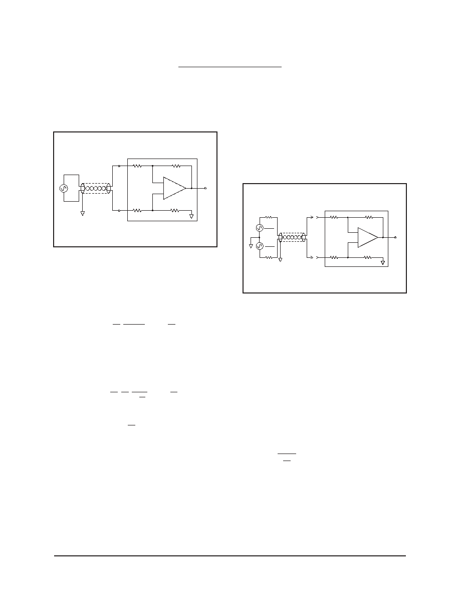
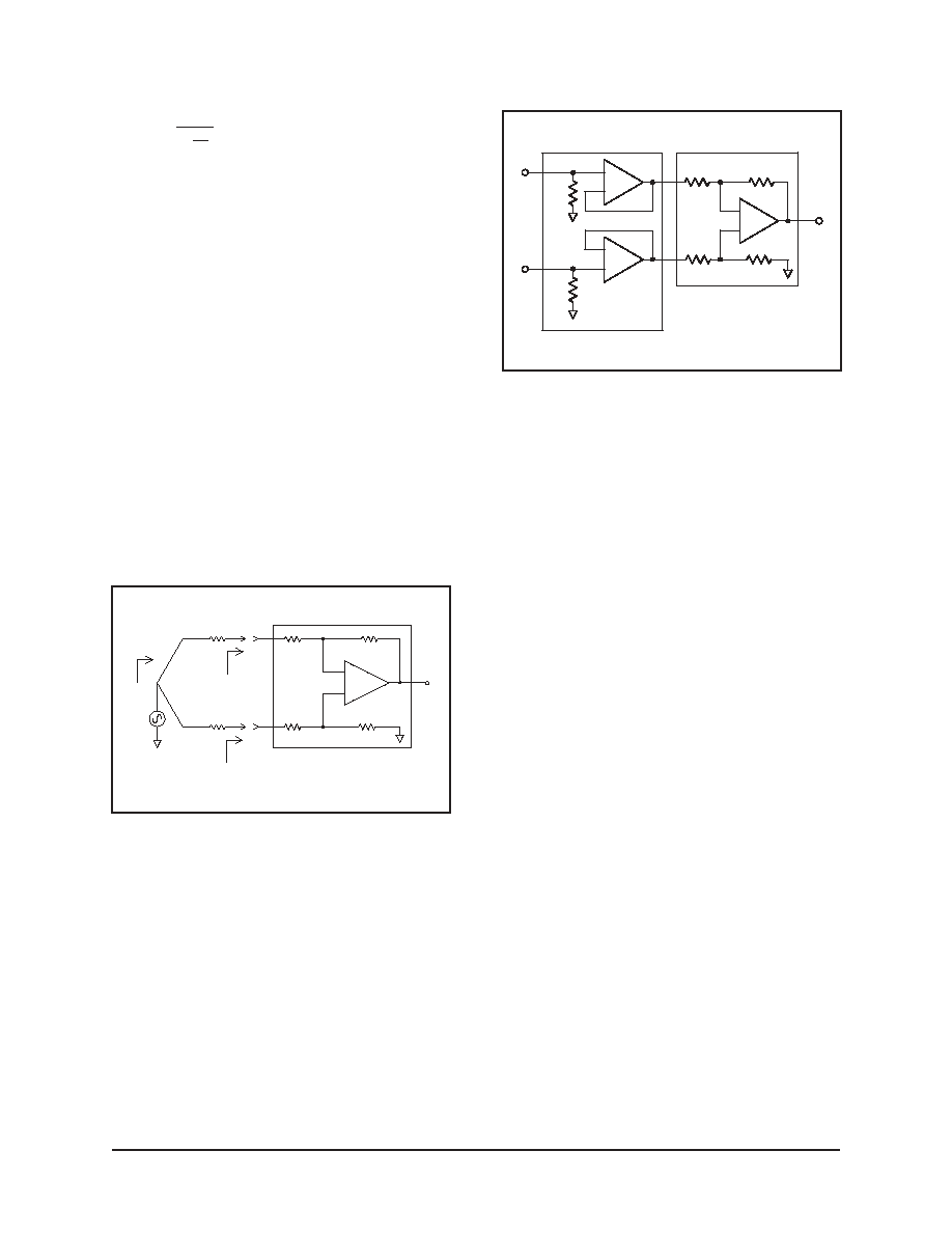
The Impact of Driving Source Impedance
However, in the real world, where sources have
non-zero output impedance, the situation is more
complicated. Figure 4 shows the equivalent circuit of
a real-world differential application. In this case, the
source connected to the differential receiver has
source impedance of R
s+
in the positive side, and R
s-
in the negative side. Because these two resistive ele-
ments are in series with each other, they only serve to
attenuate the signal V
diff
relative to the input imped-
ance of the differential stage. Even if they (Rs+ and
Rs-) are mismatched, this attenuation is the only con-
sequence of non-zero source impedance.
However, the same cannot be said for com-
mon-mode interference. Common-mode signals ap-
pear in phase between the two input terminals. For
in-phase signals, the source impedances can have
significant impact. As shown in Figure 5, this is be-
cause each leg of the source impedance forms a volt-
age
divider
when
it
interacts
with
the
input
impedance of its respective input of the differential
amplifier.
Because the + and - inputs of the operational am-
plifier are forced by feedback to maintain the same
voltage, the individual common-mode impedances of
each side of the differential stage are:
Z
R
R
CM +
=
+
3
4
; and
Z
CM
R
R
R
R
-
+
=
3
4
3
1
.
So long as R
1
=R
3
, these impedances, which form
a load for common-mode input signals, are identical.
(This is why, in discrete applications, it is wise to
choose R
1
=R
3
, and why, in all integrated applica-
tions, these resistors are chosen to be the same
value.)
The total common-mode input impedance is
THAT Corporation; 45 Sumner Street; Milford, Massachusetts 01757-1656; USA
Tel: +1 508 478 9200; Fax: +1 508 478 0990; Web: www.thatcorp.com
Page 4
InGenius High CMRR-Balanced Input Line Receiver IC
Vdiff
+
-
Vout
Vin+
Vin-
R1
R2
R3
R4
Figure 3. Basic differential amplifier
Rs-
Rs+
+
-
Vout
Vin+
Vin-
R1
R2
R3
R4
Vdiff
2
Vdiff
2
-
+
-
+
Figure 4. Basic differential amplifier showing
mismatched source impedances
Z
CM
R
R
R
R
=
+
+
3
4
3
1
1
.
Source Impedance Mismatches Ruin Good CMRR
Even if R
1
perfectly matches R
3
, any mismatch in
the source impedances R
S+
and R
S-
will cause the
voltage dividers to be unequal between the two input
legs. This means that V
in-
and V
in+
in Figure 5 are no
longer equal to each other. Essentially, imbalances in
the two source impedances convert the common
mode signal to a differential signal, which will not be
rejected by the input stage no matter how high its
theoretical CMRR is.
To see how this plays out in practice, consider the
case of a typical unity-gain conventional balanced line
receiver with common-mode input impedance of
10 k
. In such cases, a source impedance imbalance
of only 10
can degrade CMRR to no better than
66 dB. A 10
mismatch could be caused by toler-
ances in coupling capacitors or output build-out re-
sistors. The situation becomes much worse when a
conventional balanced line receiver is driven from an
unbalanced source, where it is common to use at
least 100
in series with the output for protection.
(With a 100
unbalanced output impedance, and a
10 k
common-mode input impedance, even a per-
fect simple input stage can provide no more than
46 dB CMRR!)
The best solution to this problem is to increase
the line receiver's common-mode input impedance
enough to minimize the unbalancing effect of the volt-
age divider. Preferably, this means achieving input
impedances on the order of several megohms. How-
ever, in a conventional differential amplifier, this re-
quires high-value resistances in the circuit.
High
resistance carries with it a high noise penalty, making
this straightforward approach impractical for quality
audio devices.
Instrumentation Amplifiers
Some designers prefer the more elaborate ap-
proach of an instrumentation amplifier, as shown in
Figure 6. In this circuit, it is possible to raise the in-
put impedance (both common-mode and differential)
of the stage because the load seen by the source is
decoupled by OA
1
and OA
2
from the balanced stage
(OA
3
along with R
1
, R
2
, R
3
, and R
4
). In this circuit,
Z
CM- = Ri1
, and Z
CM+
= R
i2
.
To retain 90 dB CMRR in the face of a 10
mis-
match in source impedance would require R
i1
and
R
i2
to be > 317 k
. Of course, any difference in the
values of R
i1
and R
i2
themselves would further unbal-
ance common mode signals as well, so these resis-
tors would ideally be trimmed just like the resistors
in the single opamp stage of Figure 3. Unfortunately
for this approach, it is difficult and expensive to
make precision trimmed resistors with such high val-
ues.
Furthermore, since the input bias current for am-
plifiers OA
1
and OA
2
flows through these resistors,
their input currents must be extremely low if they are
not to cause significant offsets. Practically, this neces-
sitates using FET input stages for OA
1
and OA
2
.
While FETs may be a viable alternative, it is difficult
to achieve with them the low noise performance of
modern bipolar input stages.
Transformer Input Stages
From the point of view of common mode input
impedance, as well as that of electrical isolation, a
transformer in front of the first active input stage is
really the best possible solution. Transformers are
the only approach of which we are aware that pro-
vides true electrical isolation with reasonable fidelity.
Furthermore, their common-mode input impedance
is easily extremely high (tens of Megohms), and al-
most completely decoupled from their differential in-
put impedance.
But, transformers have many other limitations.
They do not offer dc coupling, and suffer from satu-
ration at low frequencies unless they are physically
large and carefully made.
Again, unless they are
carefully made (which usually equates to high cost),
they introduce phase shift at high audio-band fre-
quencies.
Furthermore, they tend to be big and
heavy and pick up external magnetic fields, some-
THAT Corporation; 45 Sumner Street; Milford, Massachusetts 01757-1656; USA
Tel: +1 508 478 9200; Fax: +1 508 478 0990; Web: www.thatcorp.com
600033 Rev 00
Page 5
Vcm
Rs-
Rs+
Zcm-
Zcm+
Zcm
+
-
Vout
Vin+
Vin-
R1
R2
R3
R4
Figure 5. Basic differential amplifier driven
by common-mode input signal
Out
In-
In+
+
-
+
-
+
-
OA1
OA2
OA3
Ri1
Ri2
R1
R2
R3
R4
Figure 6. Instrumentation amplifier
times making it difficult to locate transformer-cou-
pled equipment to avoid interference.
Fortunately, audio equipment usually does not re-
quire true electrical isolation. In most cases, trans-
formers out-perform conventional input stages only
because they excel at rejecting common-mode signals
in real-world situations. It is no coincidence that the
InGenius concept was developed by an individual re-
sponsible for manufacturing the world's premier line
of audio transformers (Bill Whitlock, of Jensen
Transformers). Bill's InGenius technology offers all
the advantages of solid state input stages, including
dc coupling, negligible phase shift from dc to beyond
the edge of the audio band, and vanishingly low dis-
tortion, along with the primary advantage of a trans-
former:
extremely
high
common-mode
input
impedance.
The InGenius Approach
The InGenius approach to balanced line receivers
uses bootstrapping to increase common mode input
impedance. With bootstrapping, we first create a rep-
lica of the common mode signal, and then feed it
back appropriately to the inputs to increase the input
impedance. Because doing this in a differential
amplifier involves additional complications, it is use-
ful to review the bootstrap concept with a sin-
gle-ended design first.
We will then show how Bill
Whitlock applied that concept to the differential case.
Bootstrapping: a Simple Single-Ended Example
To illustrate the concept behind bootstrapping,
consider the the single-ended bootstrap shown in
Figure 7. In this circuit, amplifier A is configured for
unity gain, and can be considered to have infinite in-
put impedance. Capacitor C
b
blocks DC, so at DC,
the input impedance, Z
in
, is R
a
+R
b
.
However, for high-frequency AC signals (where C
b
is effectively a short), amplifier A drives the junction
of R
a
and R
b
through C
b
to nearly the same AC volt-
age as V
in
.
As a result, practically no AC current
flows through R
a
. This effectively increases the input
impedance seen at Z
in
.
The cutoff frequency of the filter formed by C
b
and R
a
/R
b
is determined primarily by the values of C
b
and R
b
. (Because so little current flows in R
a
, it is
hardly involved in this filter.)
Input impedance Z
in
; at frequency f, is described
the following equation:
Z
R
R
in
a
b
G
f
f n
f
fD
=
+
+
+ -
(
)
(
)
(
) (
)
1
1 1
2
2
2
where
f
n
C
R a Rb
R a Rb
b
=
+
1
2
(
)
f =
D
R C
b
b
1
2
For example, if R
a
and R
b
are 10 k
each, Z
inDC
is
20 k
. This resistance provides a DC path for am-
plifier bias current. At higher frequencies, the boot-
strap greatly increases the input impedance, limited
ultimately by how close gain G approaches unity.
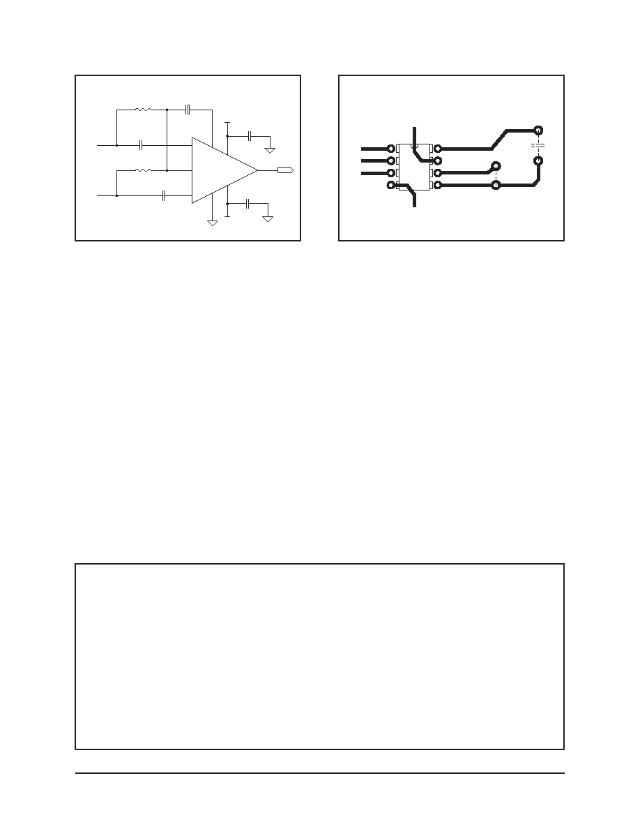
Common Mode Bootstrapping in an
Instrumentation Amplifier = InGenius
The genius behind Bill Whitlock's invention was
to recognize that in an instrumentation amplifier, it is
possible bootstrap the common-mode signal to in-
crease common-mode input impedance. This is the
concept behind the InGenius patents.
To see how
this works, refer to the circuit of Figure 8.
Like Figure 1, Figure 8 shows an equivalent cir-
cuit for the THAT 1200-series ICs. OA
1
and OA
2
are
high input-impedance, unity-gain buffers feeding dif-
ferential amplifier OA
3
in an instrumentation ampli-
fier
configuration.
OA
4
is
a
third
high
input-impedance, unity-gain buffer. With R
10
= R
11
,
the voltage at the input to OA
4
will be equal to the
common-mode component of the input signal. OA
4
buffers this signal, and feeds it back to both inputs
via capacitor C
b
and resistors R
6
, R
7
, R
8
, R
9
, and R
5
.
Note that in most applications C
b
is large (>100
µf).
THAT Corporation; 45 Sumner Street; Milford, Massachusetts 01757-1656; USA
Tel: +1 508 478 9200; Fax: +1 508 478 0990; Web: www.thatcorp.com
Page 6
InGenius High-CMRR Balanced Input Line Receiver ICs
Ra
Rb
G = 1
Cb
A
[R5]
[(R6+R7)||(R8+R9)]
Zin
Rs
V
Vin
Figure 7. Single-ended bootstrap topology
+1
+1
R1
R2
R3
R4
IN-
IN+
REF
CM OUT
Vout
+1
-
+
CM IN
Cb
R5
R7
R8
R10
R11
OA1
OA2
OA3
OA4
24K
24K
24K
R6
R9
Figure 8. THAT1200-series equivalent circuit diagram

Similarly to the single-ended application above, at
high frequencies, the junction of R
7
, R
8
, and R
5
is
driven through C
b
to the same potential as the com-
mon-mode input voltage. Hence at high frequencies,
no common-mode current flows in resistors R
6
and
R
7
, or R
8
and R
9
. Since OA
1
and OA
2
have high input
impedances, this effectively raises the input imped-
ance seen at In+ and In- to high-frequency com-
mon-mode signals. Of course, for differential signals,
the input impedance is (R
6
+R
7
+R
8
+R
9
). And, at DC,
the common-mode input impedance is:
Z
R
R
R
R
R
R
R
R
R
CM DC
=
+
+
+
+
+
+
(
)(
)
6
7
8
9
6
7
8
9
5.
DC bias for OA
1
and OA
2
is supplied through R
5
and either R
7
or R
8
.
For the resistor values chosen for the 1200-series
ICs, the input impedances Z
CM
and Z
diff
, are de-
scribed by the following equations:
Z
k
CM DC
= 36
Z
f
k
CM
C
f
C
f
b
b
( )
(
)
(
.
)
=
+
+
36
1 50240
1 73 8
2
2
; where f is the in-
put frequency,
Z
R
R
R
R
k
diff
=
+
+
+
=
6
7
8
9
48
In order to get the most out of this topology, OA
1
and OA
2
must have high input impedance, and the
common-mode gain loop (OA
1
, OA
2
, R
10
/R
11
and OA
4
)
must have precisely unity gain over the entire audio
band. THAT Corporation integrated the InGenius
parts in our complimentary dielectric isolation pro-
cess because it offers very high bandwidth and low
noise for relatively high-voltage applications like this
one. This in turn makes it easier to meet these re-
quirements, and typically, results in a maximum
mid-audio-band Z
inCM
of > 20 M
.
Because OA
1
and OA
2
isolate the differential am-
plifier (OA
3
) from the effects of external source im-
pedances, the CMRR of OA
3
and its associated four
resistors is determined solely by OA
3
's bandwidth
and the precision of the resistor matching. Our com-
plimentary DI process contributes to high bandwidth
in OA
3
, and we use on-chip laser trimming to ensure
extremely good matching, as well as precise gain, in
those four thin-film resistors.
Finally, perhaps the most common interfering sig-
nals that a good differential line receiver must reject
is the power-line frequency: usually either 50 or
60 Hz and its harmonics. So, it is essential that the
common-mode input impedance remain high down
to 50 Hz, and up to at least to the edge of the audio
band. While THAT's process and circuit design en-
sure the latter condition, the value of C
b
will deter-
mine how low in frequency the common-mode input
impedance will be increased. To maintain at least a
1 M
common-mode input impedance, C
b
should be
at least 10
µf.
It is possible to solve the above equation for C
b
in
terms of the desired Z
CM
for a specific frequency.
However, reaching a general closed-form solution is
difficult and results in a very complex formula. The
relatively simple formula below takes advantage of
some approximation, and yields good results for Z
CM
between about 100 k
and 10 M.
C
b
Z
f
CM
◊
-
0 553 10
3
.
THAT Corporation; 45 Sumner Street; Milford, Massachusetts 01757-1656; USA
Tel: +1 508 478 9200; Fax: +1 508 478 0990; Web: www.thatcorp.com
600033 Rev 00
Page 7
For additional information refer to:
Balanced Lines in Audio Systems - Fact, Fiction, and Transformers, by Bill Whitlock, AES 97th Convention,
Preprint 3917, October 1994
A New Balanced Audio Input Circuit for Maximum Common-mode Rejection in Real-world Environments, by
Bill Whitlock, AES 101st Convention Preprint 4372, 1996.
Common-Mode to Differential-Mode Conversion in Shielded Twisted-pair Cables (Shield-Current-Induced
Noise), by Jim Brown & Bill Whitlock, AES 114th Convention, Preprint 5747, February 2003
Applications
Basic Application
At its most basic, THAT's 1200-series ICs need
very little external support circuitry. As is shown in
the basic application circuit of Figure 9, they need lit-
tle else beyond positive and negative power supplies,
a ground reference, the common-mode bootstrap ca-
pacitor, and input and output connections. Because
all 1200-series ICs are wide bandwidth parts, it is
important to provide bypass capacitors for both posi-
tive and negative supply rails within an inch or so of
the part.
Sharing supply bypass capacitors across
several 1200-series ICs separated by several inches
on a circuit board (as, for example, along the back
panel of a multi-input product) is not recom-
mended
1
.
Bootstrap Capacitor Polarity
Because the bootstrap capacitor, C
b
, will usually
be large (see formula on page 7) an electrolytic or
tantalum capacitor is a logical choice. Such capaci-
tors are normally polarized, though non-polarized
types
are
available
at
higher
cost.
For
the
1200-series, a polarized capacitor is appropriate,
with the positive end towards CM
out
(pin 8), because
of the direction of the input bias currents for internal
opamps OA
1
and OA
2
. Furthermore, because C
b
never has much voltage across it
2
, it only needs to
support a few tens of mV. Therefore, we recommend
a 220 uF, 3V capacitor for C
b
.
RFI Protection
3
As an input stage, the 1200-series ICs are suscep-
tible to RF interference (RFI). Like most semiconduc-
tor devices, if high levels of RF are permitted at the
input pins of 1200-series parts, they may become
nonlinear, which can create audible interference.
Therefore, it is good design practice to filter un-
wanted high frequencies at the input of any product
in which the 1200-series is used.
The objective
should be to prevent RF from entering the chassis,
and especially, the circuit board of any devices using
a 1200-series part. Generally, this is done by means
of small capacitors connected between the signal in-
puts and chassis ground, with the capacitors located
as physically close to the input connectors as possi-
ble.
Figure 10 shows a basic, simple application cir-
cuit to protect the 1200 series against RFI. For many
non-demanding applications, this simple circuit will
suffice. C
1
and C
2
provide RF bypassing from pins 2
and 3 of the input XLR connector to chassis ground
and the XLR connector's shell (which are tied to-
gether, ideally only at the XLR connector jack). RF
picked up on the cable plugged into the connector is
conducted by C
1
and C
2
to chassis ground. Chassis
ground should connect to circuit ground through one
(and only one) low inductance path, usually at the
power supply connector.
THAT Corporation; 45 Sumner Street; Milford, Massachusetts 01757-1656; USA
Tel: +1 508 478 9200; Fax: +1 508 478 0990; Web: www.thatcorp.com
Page 8
InGenius High-CMRR Balanced Input Line Receiver ICs
U1
Vcc
Vee
C4
100nF
C3
100nF
In-
In+
5
IN-
2
IN+
3
8
4
1
7
6
OUT
CM
IN
CM
OUT
REF
Vcc
Vee
Cb
220uF
OUT
+
120X
Figure 9. Basic 1200-series application circuit
U1
Vcc
Vee
C4
100nF
C3
100nF
5
IN-
2
IN+
3
8
4
1
7
6
OUT
CM
IN
CM
OUT
REF
Vcc
Vee
Cb
220uF
5 4
3 1
2
2
3
1
J1
XLR-F
OUT
C2
100pF NPO
C1
100pF NPO
+
120X
Figure 10. THAT1200 application with
simple RFI protection
1
Lack of proper bypassing may not cause obvious problems at normal temperatures. We have seen cases in which improperly bypassed parts begin
to draw excessive current when operated near their upper temperature limits. Close bypassing prevents this phenomenon.
2
Even at DC, C
b
will not see much voltage, because the signal at the junction of R
7
and R
8
should closely equal the signal at the junction of R
10
and
R
11
. With OA
4
configured for unity gain, both ends of C
b
see the same signal - AC and DC - except for offsets.
3
Good practice to protect inputs against RFI is a science in itself, and it is beyond the scope of this data sheet to provide more than a glimpse of this
complex subject. We refer the interested reader to:
Considerations in Grounding and Shielding Audio Devices, by Stephan R. Macatee, JAES Volume 43, Number 6, pp.472-483; June 1995;
Noise Susceptibility in Analog and Digital Signal Processing Systems, by Neil A. Muncy, AES 97th Convention Preprint 3930, October 1996.
The one drawback to this circuit is that C
1
and C
2
will reduce the common-mode input impedance of
the 1200 stage to ~ 80 k
at 20 kHz. Of course, this
figure drops by a factor of ten for each decade in-
crease in frequency. Additionally, any mismatch be-
tween these capacitors can unbalance an interfering
common-mode signal, thus making it impossible for
the 1200 to reject it.
Figure 11 shows a more elaborate and robust cir-
cuit for RFI protection. While more complex, it offers
many improvements over the circuit of Figure 10 that
make it worth serious consideration. First, C
1
and C
2
are larger than their counterparts in Figure 10. Be-
cause they are in series with each other, they act as a
235 pf capacitor across pins 2 and 3 of the XLR.
This allows them to be effective at lower frequencies.
Second, because their center point ties to chassis
ground through a smaller, common capacitor (C
3
,
100 pf), any mismatch in their values has less ten-
dency to unbalance common-mode signals compared
to the circuit of figure 10
4
. Third, because they are
driven from the common-mode bootstrap circuit
through R
3
, this common point gains the benefit of
the InGenius common-mode bootstrapping. Finally,
R
1
and R
2
provide some additional buildout imped-
ance against which the bypass capacitors can work,
making the entire network more effective against
strong RF signals.
ESD Protection
All
the
1200-series
ICs
contain
internal
over-voltage protection circuitry for the two input
pins. Figure 12 is an equivalent circuit of this cir-
cuitry.
These internal diodes provide modest protection
against common low-voltage ESD incidents.
How-
ever, because these ICs are intended to be connected
directly
to
the
input
connectors
of
electronic
products, they may be exposed to unpredictable and
possibly extreme ESD.
For ESD to affect the
InGenius operation, it would have to be conducted
via one of the input connectors to the device itself.
This is unlikely, but certainly not impossible. Not
surprisingly, THAT's own testing indicates that re-
peated exposure to high levels (above 1 kV) of ESD
through pins 2 and/or 3 of the input XLR connector
can adversely affect the device's CMRR, and may
cause failure if the ESD reaches sufficiently high lev-
els.
If the application requires surviving such ESD in-
cidents, THAT recommends the circuit of either Fig-
ure 13 or 14. Figure 13 is appropriate for the 1203
and 1206, both of which support input signals that
swing higher than the supply rails. This arrangement
of signal and Zener diodes permits the maximum al-
lowable (audio) input signal to reach the IC's input
THAT Corporation; 45 Sumner Street; Milford, Massachusetts 01757-1656; USA
Tel: +1 508 478 9200; Fax: +1 508 478 0990; Web: www.thatcorp.com
600033 Rev 00
Page 9
5
IN-
2
IN+
3
8
4
1
7
6
OUT
CM
IN
CM
OUT
REF
Vcc
Vee
U1
R3
4k7
Cb
220uF
C1
470pF
C2
470pF
C3
100pF
R1
R2
5 4 3 1
2
2
3
1
J1
XLR-F
Vcc
Vee
OUT
100R
100R
(see text)
+
C5
100nF
C4
100nF
120X
Figure 11. THAT1200 application with recommended RFI protection.
Ra
Rb
Rc
Rd
Vcc
Vee
Vee
IN+
IN-
CM IN
Vcc
Figure 12. Internal input protection circuitry
4
For additional information refer to the publications listed on page 7.
pins, but directs high-energy ESD impulses to the
rails. So long as the supply rails are adequately de-
coupled and the diodes themselves are reasonably
robust, all but the most drastic ESD events will not
affect the 1203/6 IC itself. Figure 14, which works
similarly, is appropriate for the 1200, which is lim-
ited to input signals up to about the supply rails.
D
1
through D
4
in figures 13 and 14 can be
1N4148 types, while the 12V Zener diodes should be
Ω watt to allow them to support relatively high cur-
rents with 12V across them for the short duration of
an ESD pulse.
We will continue to work to find real world solu-
tions to the often difficult problem of ESD protection.
Please look to our web site for future application
notes regarding this subject.
Note that we know of no circuit that will protect
against really strong ESD, such as lightning, so
please do not take this advice as suggesting that the
circuits of Figures 13 and 14 are completely immune
to ESD!
AC Coupling Inputs
It is not necessary to AC couple the 1200-series
inputs. However, if desired, we recommend the cir-
cuit of Figure 15. In this circuit Resistors R
1
and R
2
benefit from the common-mode bootstrap via their
connection to CM
in
. This reduces their impact on
common-mode input impedance, preserving the ben-
THAT Corporation; 45 Sumner Street; Milford, Massachusetts 01757-1656; USA
Tel: +1 508 478 9200; Fax: +1 508 478 0990; Web: www.thatcorp.com
Page 10
InGenius High-CMRR Balanced Input Line Receiver ICs
Vcc
Vee
D5
12V
D6
12V
D2
D1
D4
D3
5
IN-
2
IN+
3
8
4
1
7
6
OUT
CM
IN
CM
OUT
REF
Vcc
Vee
U1
R3
4k7
Cb
220uF
C1
470pF
C2
470pF
C3
100pF
R1
R2
5 4 3 1
2
2
3
1
J1
XLR-F
Vcc
Vee
OUT
100R
100R
(see text)
RFI protection
+
C5
100nF
C4
100nF
1203 or
1206
ESD protection
Figure 13. RFI and ESD protection for the 1203 and 1206
Vcc
Vee
D2
D1
D4
D3
5
IN-
2
IN+
3
8
4
1
7
6
OUT
CM
IN
CM
OUT
REF
Vcc
Vee
U1
R3
4k7
Cb
220uF
C1
470pF
C2
470pF
C3
100pF
R1
R2
5 4 3 1
2
2
3
1
J1
XLR-F
Vcc
Vee
OUT
100R
100R
(see text)
RFI protection
+
C5
100nF
C4
100nF
ESD protection
1200
Figure 14. RFI and ESD protection for the 1200
efit of InGenius, while providing a discharge path for
charge in the input coupling capacitor. Choose capac-
itors large enough to present minimal impedance to
the lowest signals of interest, compared to the differ-
ential input impedance of the InGenius IC (48 k
). If
desired, this may be combined with the RF protec-
tion of Figures 10 or 11, and ESD protection of fig-
ures 13 or 14.
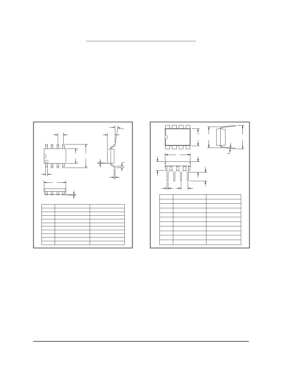
Dual Layout Option
InGenius ICs are available only from THAT Cor-
poration.
Should a manufacturer wish to provide
some alternatives to the 1200 series, it is possible to
lay out the circuit board for a 1200 such that a THAT
1240-series
(conventional)
balanced
input
stage
could be substituted in a pinch. Since the 1240 se-
ries is pin-compatible with similar parts available
from other manufacturers, this offers the possibility
of several reduced-performance second sources if
1200-series ICs were for unavailable for any reason.
The PCB layout shown in Figure 16 provide man-
ufacturers with the option to load a PCB with either
of these input stages. Note that these figures are not
to scale. The interconnects should be as short as
practical, constrained only by component size and
relevant manufacturing considerations.
When a THAT 1200-series IC is installed, capaci-
tor C
b
is connected between CM
in
and CM
out
. No con-
nection is made between V
out
and CM
in
. When the
THAT 1240-series is used, capacitor C
b
is removed,
and a jumper connects the V
out
and Sense pins.
THAT Corporation; 45 Sumner Street; Milford, Massachusetts 01757-1656; USA
Tel: +1 508 478 9200; Fax: +1 508 478 0990; Web: www.thatcorp.com
600033 Rev 00
Page 11
U1
Vcc
Vee
C4
100nF
C3
100nF
In-
In+
C1
10uF
R1
100k
C2
10uF
5
IN-
2
IN+
3
8
4
1
7
6
OUT
CM
IN
CM
OUT
REF
Vcc
Vee
Cb
220uF
OUT
+
120X
R2
100k
Figure 15. AC coupling 1200-series inputs
Vcc
Gnd
In-
In+
Vee
CM out or N/C
Vcc
Vout
CM in or Sense
Short only for
THAT1240-series
Ref
In-
In+
Vee
Cb
THAT1200-series
or THAT1240-series
+
load only for
THAT1200-series
Figure 16. Dual PCB layout for THAT120X and THAT124X
Information furnished by THAT Corporation is believed to be accurate and reliable. However no responsibil-
ity is assumed by THAT Corporation for its use nor for any infringements of patents or other rights of third par-
ties which may result from its use.
LIFE SUPPORT POLICY
THAT Corporation products are not designed for use in life support equipment where malfunction of such
products can reasonably be expected to result in personal injury or death. The buyer uses or sells such prod-
ucts for life suport application at the buyer's own risk and agrees to hold harmless THAT Corporation from all
damages, claims, suits or expense resulting from such use.
CAUTION: THIS IS AN ESD (ELECTROSTATIC DISCHARGE) SENSITIVE DEVICE.
It can be damaged by the currents generated by electrostatic discharge. Static charge and therefore danger-
ous voltages can accumulate and discharge without detection causing a loss of function or performance to occur.
Use ESD preventative measures when storing and handling this device. Unused devices should be stored in
conductive packaging. Packaging should be discharged before the devices are removed. ESD damage can occur
to these devices even after they are installed in a board-level assembly. Circuits should include specific and ap-
propriate ESD protection.
Package and Soldering Information
The THAT 1200 series is available in both 8-pin
mini-DIP and 8-pin SOIC packages. The package di-
mensions are shown in Figures 17 and 18 below,
while pinouts are given in Table 1 on page 1.
The 1200 series is available only in lead-free,
"green" packages (both SO and DIP). The lead frames
are copper, plated with successive layers of nickel
paladium, and gold. This approach makes it possible
to
solder
these
devices
using
lead-free
and
lead-bearing solders. The plastic mold compound
contains no hazardous substances as specified in the
RoHS directive.
The surface-mount package has been qualified
using reflow temperatures as high as 260
∞C for 10
seconds. This makes them suitable for use in a 100%
tin solder process. Furthermore, the 1200 series has
been qualified to a JEDEC moisture sensitivity level
of MSL1. No special humidity precautions are re-
quired prior to flow soldering the parts.
The through-hole package leads can be subjected
to a soldering temperature of 300 ∞C for up to 10 sec-
onds.
THAT Corporation; 45 Sumner Street; Milford, Massachusetts 01757-1656; USA
Tel: +1 508 478 9200; Fax: +1 508 478 0990; Web: www.thatcorp.com
Page 12
InGenius High-CMRR Balanced Input Line Receiver ICs
0.41/0.89
0.31/0.71
H
h
0.016/0.035
0.012/0.027
0.230/0.244
0.007/0.010
0.060/0.068
0.014/0.018
0.188/0.197
0.004/0.008
INCHES
0.150/0.157
G
H
F
C
B
D
F
G
D
E
A
a1
B
C
ITEM
MILLIMETERS
0.36/0.46
0.18/0.25
1.52/1.73
1.27
4.78/5.00
0.10/0.20
3.81/3.99
5.84/6.20
0.050
A
E
a1
0-8∞
hx45∞
1
Figure 17. -S (SO) version package outline drawing
B
A
K
F
H
E
D
G
J
C
ITEM
A
B
C
D
E
F
G
H
J
K
1
MILLIMETERS
9.52 0.10
6.35 0.10
7.49/8.13
0.46
2.54
3.68/4.32
0.25
3.18 0.10
8.13/9.40
3.30 0.10
±
±
±
±
INCHES
0.375
0.250 0.004
0.295/0.320
0.018
0.100
0.145/0.170
0.010
0.125 0.004
0.320/0.370
0.130 0.004
±0.004
±
±
±
Figure 18. -P (DIP) version package outline drawing